The Apollo program was never really about the moon. It was about what the act of reaching for the moon produced along the way: breakthroughs in materials science, computing, telecommunications, and manufacturing that transformed civilian life for decades after the last astronaut came home. The mission was the catalyst for these revolutionary technologies.
Something similar is happening in Japan right now. And it started with the country’s worst disaster.
Blind Inside A Melting Reactor
On March 11, 2011, a magnitude 9.0 earthquake and tsunami triggered three reactor meltdowns at the Fukushima Daiichi Nuclear Power Plant. It was the worst nuclear accident since Chernobyl. But there was a second failure that received less attention: inside the reactors, every sensor, every monitoring circuit, every electronic system was destroyed. Not by the earthquake or the water, but by the heat and radiation that followed.
Silicon, the material that powers virtually all modern electronics, cannot function in those conditions. Workers were forced into the most dangerous phase of the crisis with almost no data about what was happening inside the reactors they were trying to save.
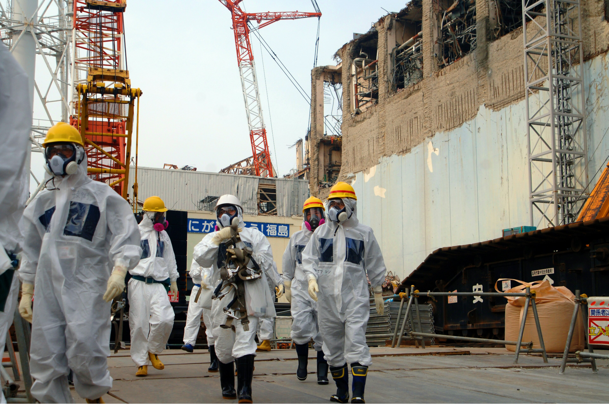
That electronic blindness persists to this day. While progress has been made, measurement in such harsh environments remains highly constrained. More than 880 tons of fuel debris—molten mixtures of nuclear fuel and structural materials— remain inside the damaged reactors. The most technically difficult decommissioning operation in history, safely extracting that debris, cannot proceed until instruments can survive long enough inside the reactor to gather the data needed to plan the removal. Conventional electronics still cannot do it.
The question became: is there any material that can?
The Ultimate Semiconductor That Nobody Could Build
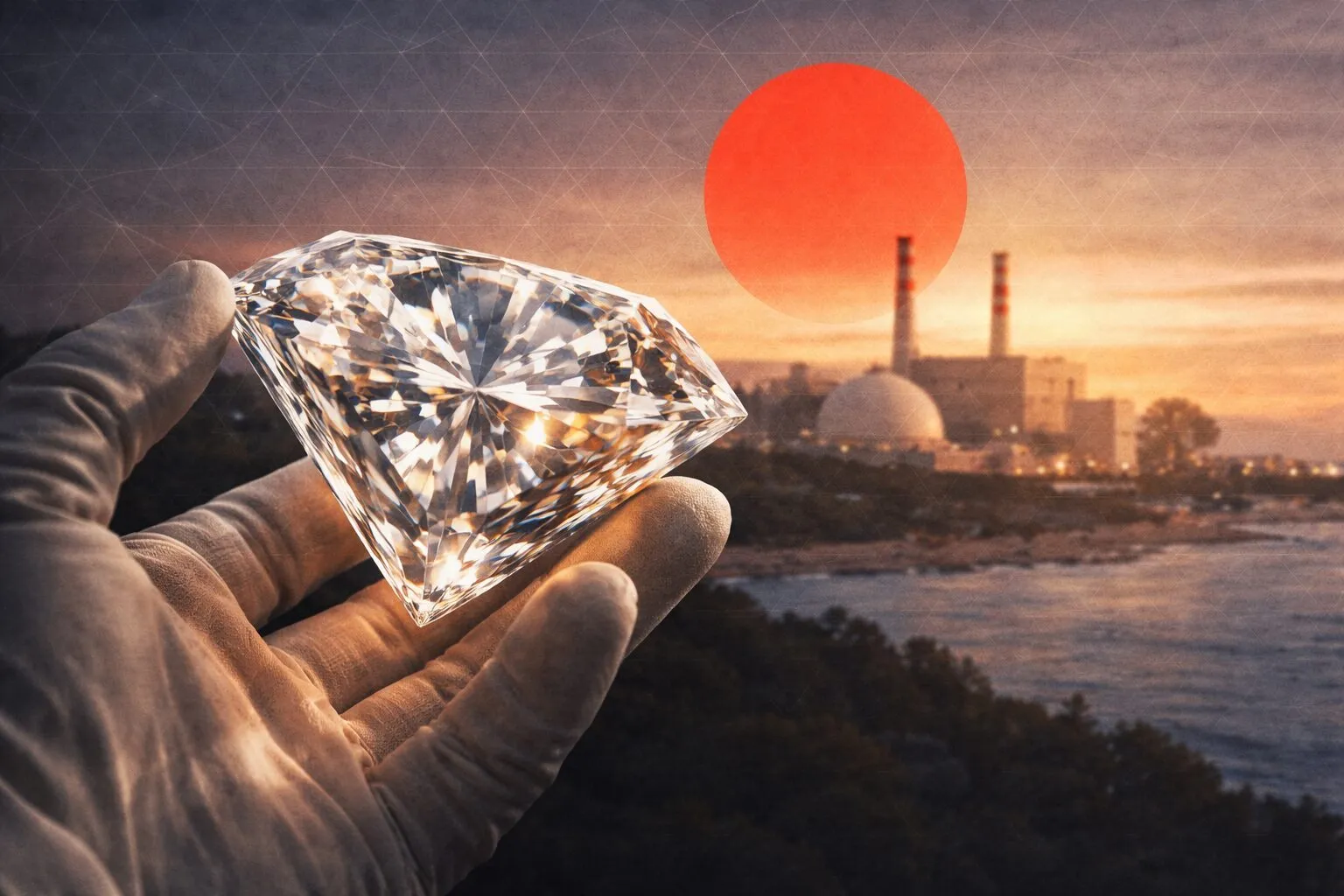
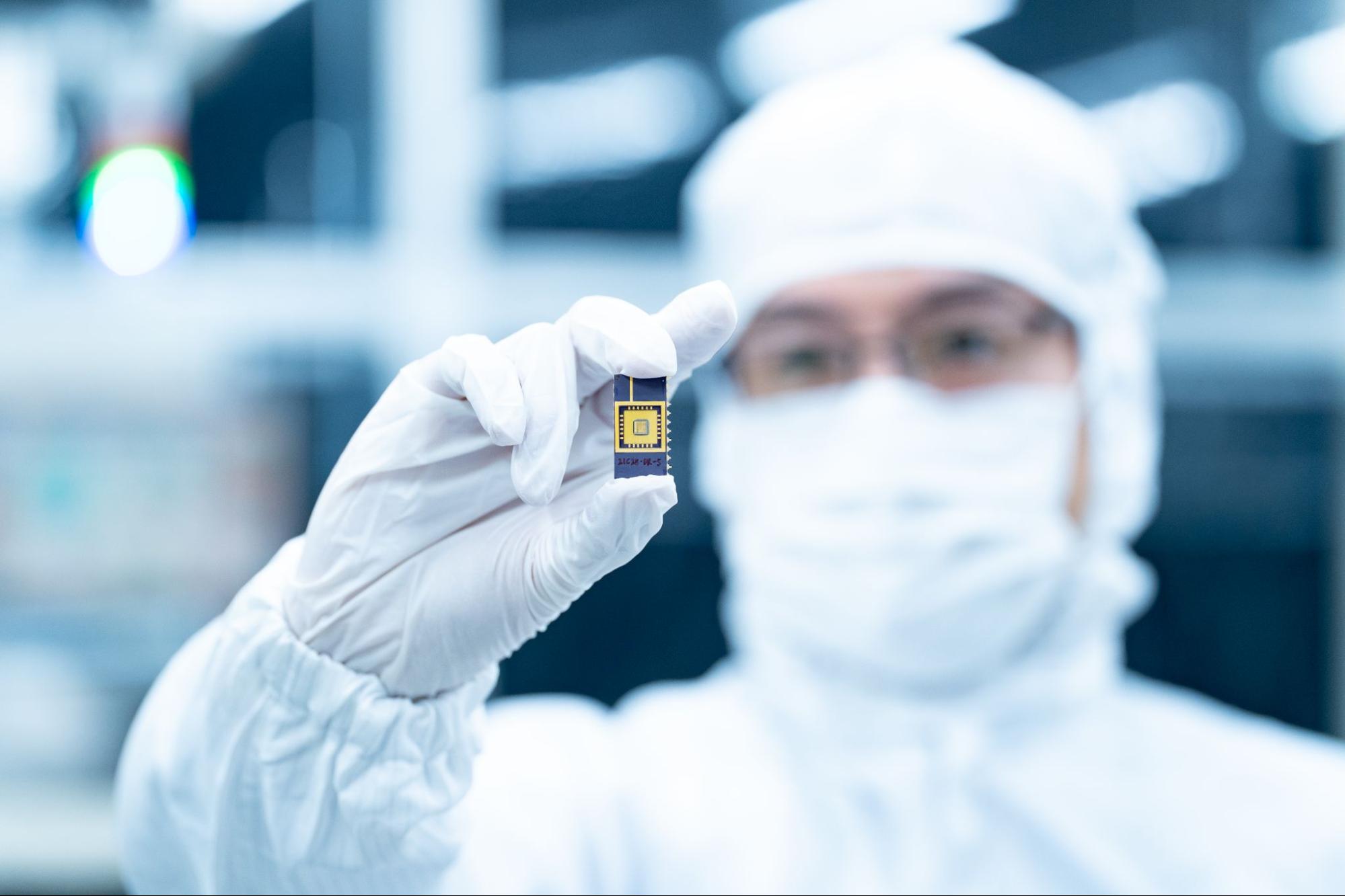
For decades, researchers have known the answer is diamond. Not as a gemstone, but as a semiconductor material. Diamond has one of the highest thermal conductivity of any known material. It handles extreme voltages with minimal power loss. It operates at temperatures far beyond the limits of silicon. And radiation that destroys conventional electronics in seconds has far less impact on diamond.
It is the ultimate semiconductor. Not the kind in your phone, which processes information, but the kind that handles raw power: converting it, amplifying it, and controlling it. These power and analog semiconductors are embedded in everything from electric vehicles to radar systems to telecommunications infrastructure.
But knowing diamond should work and actually building a diamond semiconductor device are separated by an enormous gap. For over thirty years, research labs around the world produced impressive results under ideal conditions, what insiders call “champion data,” but nothing that could be manufactured reliably at any meaningful scale. The science was proven, but the engineering was not.
Fukushima closed this gap by imposing a constraint that reoriented an entire field.
The Constraint That Changed Everything
After the disaster, the Japanese government assembled a national research project with a single objective: build semiconductor devices that could function inside a damaged nuclear reactor. Specifically, a neutron detector small enough to mount on the tip of a robotic arm, thread through narrow penetration ports into the reactor vessel, and measure neutron levels near the fuel debris to determine whether a re-criticality event, an uncontrolled chain reaction, is at risk.
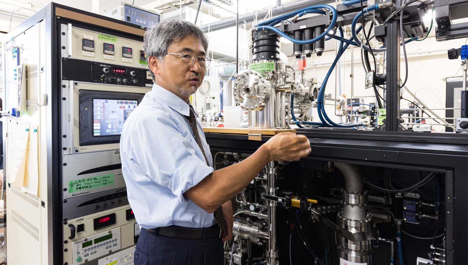
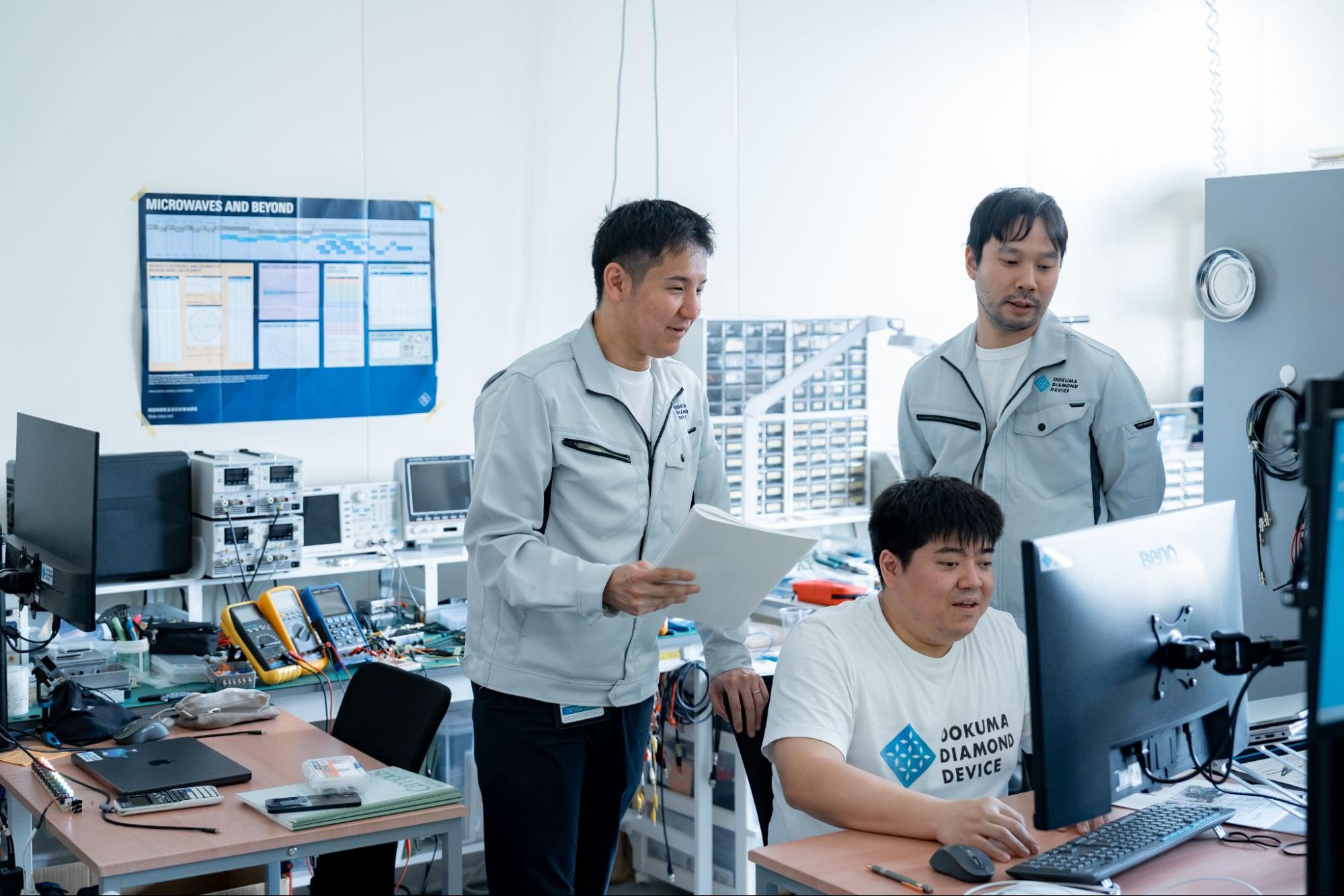
The project brought together Japan’s leading institutions: AIST, JAEA, KEK, NIMS and Hokkaido University. At its center were two researchers who had devoted their careers to diamonds. Junichi Kaneko at Hokkaido University, who also served as a visiting researcher at JAEA’s decommissioning center. And Hitoshi Umezawa at AIST, the author of what is essentially the only textbook on diamond semiconductors and one of the most cited researchers in the field globally.
But what made this project transformative was not just the caliber of the team, but the mission demanded of them.
In academic research, the incentive is to optimize for peak performance: achieve the best possible result under ideal conditions, publish, and move on. The decommissioning project demanded the opposite. These devices had to work reliably, repeatedly, in the worst environment on Earth. The question was not “what can diamond semiconductors theoretically achieve?” but “can they be manufactured consistently enough to be trusted when failure means a nuclear chain reaction?”
That shift, from optimizing performance to optimizing yield, turned out to be the decisive insight. It is the difference between proving a material works and proving it can be produced. And it gave the Japanese team a fundamental advantage over every other diamond semiconductor effort in the world, almost all of which remained oriented toward laboratory benchmarks rather than manufacturing reality.
Six Years In The Hallway
In 2016, a young serial entrepreneur named Naohisa Hoshikawa walked into Kaneko’s research lab at Hokkaido University.
Hoshikawa had already built and run a company, seizing a market created by regulatory change. The business worked. But he left it because he wanted to build something that mattered at a different scale, technology that could reshape an entire industry rather than exploit a temporary gap.
At Hokkaido University, he found a body of research that had been quietly advancing for over a decade: world-class researchers, a clear first application backed by the government, and a material whose properties opened doors to markets the researchers themselves had not yet mapped. It was the kind of opportunity that almost never exists, where deep science, commercial potential, and national priority converge.
Most founders would have incorporated immediately. Hoshikawa did not. He spent six years learning the physics. He built trust with researchers who had no reason to trust a businessman. He mapped the downstream markets. He waited for the technology to reach the point where commercialization was honest, not premature.
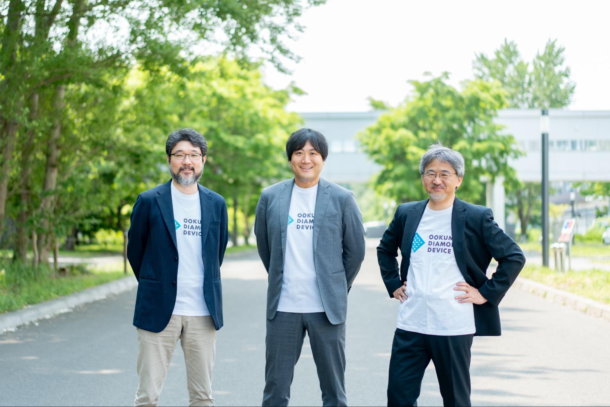
Then in March 2022, he founded Ookuma Diamond Device, with Kaneko and Umezawa as co-founders. The time had come.
The name is a statement of purpose. Okuma is the town in Fukushima Prefecture where the Daiichi plant sits. It is also where the company is building the world’s first diamond semiconductor factory.
A Technology That Outgrew Its Origin
The decommissioning mission gave Ookuma Diamond its engineering discipline and its moral foundation. But the technology it produced reaches far beyond nuclear cleanup.
Diamond semiconductors turn out to be exceptionally good at something the defense industry needs urgently: amplifying high-frequency signals at high power with far better heat dissipation.
Consider what that means for defense radar systems, such as in fighter jets. Today, radar modules use gallium nitride semiconductors that generate so much heat they require onboard liquid-cooling systems. Those systems degrade overall SWaP (Size, Weight, and Power) or otherwise constrain radar performance. Replace the gallium nitride with diamond, and the cooling system can be minimized. Radar range extends dramatically, while overall system SWaP is reduced. This enables higher performance, more flexible radar systems, supporting earlier detection of emerging threats such as drones.
Radar modules are replaced on a regular maintenance cycle and built to standardized form factors. A diamond-based module engineered to the same dimensions can be swapped in as a replacement part. No platform redesign required.
This matters now because the world has changed. Global defense spending has reached levels not seen since the Cold War. Japan’s own defense budget has roughly doubled in three years. The 21st century Space Race is commencing. The US-Japan alliance is evolving from a security relationship into an industrial one, with Japanese-founded companies beginning to serve as prime contractors on American defense programs. The infrastructure for allied co-production is being built in real time.
Diamond semiconductor technology fits this moment with unusual precision: manufactured entirely from methane gas, with no dependence on rare earths or supply chains controlled by geopolitical adversaries. Fully domestic production, in a US treaty ally. Developed over 25 years by Japanese researchers, hardened by one of the most demanding real-world engineering challenges imaginable. Ookuma Diamond has already been selected for multi-year commissioned research by the Japanese Defense Ministry. International defense investors have taken notice.
Why This Could Only Come From Japan
We spend a lot of time thinking about what we call the Japan Advantage: the structural reasons certain companies and technologies can only emerge from this country. Ookuma Diamond is one of the clearest cases we have encountered.
Start with what it takes to actually manufacture a diamond semiconductor. Most people do not realize it is an artisanal process. If there is a country where the systematization of manufacturing craft is a national tradition rather than a novel idea, it is Japan. This is where Japan’s monozukuri strengths shine. You need people who believe the quality of the 87th step matters as much as the first. That workforce exists here, and essentially nowhere else.
To add, excluding China, there are just over 100 active diamond semiconductor researchers worldwide. Ookuma Diamond employs roughly a quarter of them, including the two most cited scientists in the field globally. This concentration was built over 25 years of sustained government investment in materials science. It cannot be replicated by a well-funded competitor on any short timeline. The knowledge is too deep, too specialized, and too dependent on hands-on experience that exists only in specific labs in Sapporo and Tsukuba.
Japan is also one of the strongest countries in power and analog semiconductors, the exact category where diamond offers the greatest advantage. Mitsubishi Electric, Fuji Electric, Toshiba, and Rohm all rank among the global top ten. The industrial ecosystem to absorb this technology already exists.
Turning Adversity Into Prosperity
There is a word in Japanese, 復興, pronounced “fukko,” that is usually translated as “reconstruction” or “recovery.” That translation misses something important. Fukko does not mean restoring what existed before. It means building something new from what was lost.
The town of Okuma was evacuated in 2011. For years, it was a symbol of what the nuclear disaster had taken away. Now it is getting its first new industrial facility: a semiconductor factory, the first of its kind anywhere in the world, built to manufacture a material that humanity has tried and failed to commercialize for four decades. On March 27, 2025, more than 70 officials gathered in Okuma for the groundbreaking: the town’s mayor, a vice-minister from METI, representatives from TEPCO and Tohoku Electric Power. The facility is scheduled to begin operations in 2026, creating the first new industrial jobs in a town that is only now coming back to life.
The technology born from the crisis inside those reactors, engineered to survive conditions no other material could withstand, turns out to be the same technology the world needs to build longer-range radar, faster communications networks, and more capable satellites.
This is the pattern that defines consequential technology. Not a solution designed for a market, but a capability forged by necessity that finds markets its creators never anticipated. The Apollo program produced integrated circuits not because NASA was trying to build computers, but because the guidance systems for lunar modules needed them. Fukushima’s decommissioning challenge produced diamond semiconductors not because anyone was trying to build better radar, but because a melting reactor demanded electronics that nothing else could provide.
The factory rising in Okuma Town is the physical proof that the transition from crisis response to industry creation is underway. What began as Japan’s worst disaster may become the origin of its next great technology export.
That is what fukko looks like.
Coral Capital is an investor in Ookuma Diamond Device. Our original investment thesis is here.