Japan lost the semiconductor war thirty years ago, so they say. The narrative repeated in boardrooms from Silicon Valley to Shenzhen goes like this: In the 1980s, Japan was the “industrial superpower” that terrified Washington. By the 2000s, it had missed the digital era, crushed by the Plaza Accord and its own corporate sclerosis, while South Korea and Taiwan ate its lunch. Japan became “Galapagos”: isolated, weird, and irrelevant. The prevailing wisdom suggests that the sun set on Japanese tech dominance when the bubble burst in 1991, leaving behind a museum of hardware giants slowly rusting into obsolescence.
But there’s more to the story…
Japan never actually left. It simply retreated into the supply chain. While the world focused on who was designing the chips (Silicon Valley) or printing them (Taiwan), Japan quietly cornered the market on the “black box” technologies required to make them exist. You cannot manufacture a leading-edge chip today without Japanese photoresists, Japanese wafer cutters, or Japanese mask inspection gear. Japan didn’t lose. It specialized. It traded the low-margin glory of final assembly for the high-margin hegemony of Monozukuri (craftsmanship).
But now, the market is shifting again. We are at an inflection point. The geopolitical architecture that allowed Taiwan to become the sole foundry for global democracy is looking brittle. The “Silicon Shield” is looking less like a shield and more like a target. The world needs a backup drive. And surprisingly, the coordinates for that backup drive are pointing to a snowy plain in Northern Japan.
This is less a story about Japan “catching up” and more a story about opportunity. It is about a combination of geopolitical tailwinds, energy arbitrage, and a realization by the Japanese state that has created the conditions for a massive structural pivot.
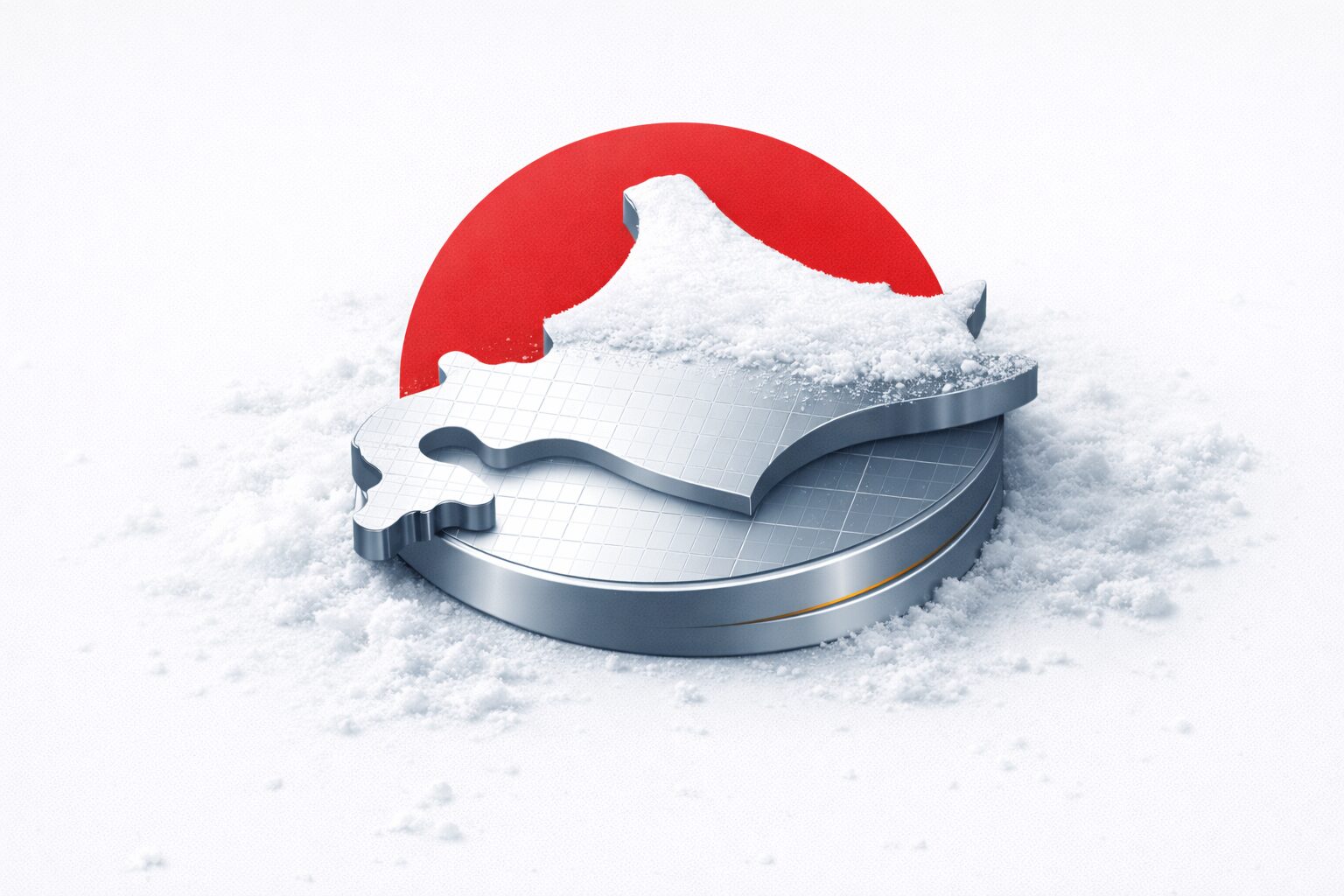
Hokkaido is the new Taiwan, thanks to a new project underway called “Rapidus.” It is the only location on the map that offers the water, the power, the talent, the culture, and the political stability to serve as the redundant node for the Western world’s computing infrastructure.
A History Lesson on Japan’s Chip Dominance
To understand why Rapidus, the government-backed consortium aiming for 2-nanometer chips, is even plausible, you have to unpack the “Japan is dying” narrative. The conventional wisdom is that Japan’s semiconductor industry collapsed because it couldn’t compete. But if you look closely at the data, the collapse was limited to specific parts of the stack.
In the late 1980s, Japan’s semiconductor market share was over 50%. NEC, Toshiba, and Hitachi were the titans of industry. They dominated DRAM (memory), the “crude oil” of the early compute era. The sheer volume of Japanese production was so overwhelming that it triggered a panic in Washington. The US response was not subtle. The 1986 US-Japan Semiconductor Agreement was essentially a managed trade deal designed to force Japan to stop “dumping” chips and open its market to US competitors.
Japan capitulated. But the real killer wasn’t the trade deal. It was the Innovator’s Dilemma.
Japanese firms were vertically integrated giants, or keiretsu. They made the chips, the vacuum cleaners, the nuclear power plants, and the heavy machinery. When the market shifted from DRAM (a commodity manufacturing game) to Logic (a design and software game) in the 1990s, Japan kept optimizing for manufacturing yield. They perfected the hardware while Silicon Valley (Intel) and Taiwan (TSMC) rewrote the software of the industry. The “foundry model” of separating design from manufacturing was heresy to the Japanese mindset. Why would you design something you didn’t build?
As Chris Miller notes in Chip War, “Japan’s companies were out-innovated not in manufacturing, but in business models.”
So Japan lost the logic market. Its share plummeted from 50% to under 10%. The memory market followed, largely ceded to Samsung and SK Hynix in Korea, who applied the Japanese model of massive capital expenditure but with faster decision loops and lower costs.
But here is the lesser known fact: Japan retreated up the stack.
Instead of fighting a losing war on commoditized chips against South Korea’s Samsung, Japanese firms focused on the equipment and materials that are difficult to commoditize because they rely on tacit knowledge, or Monozukuri.
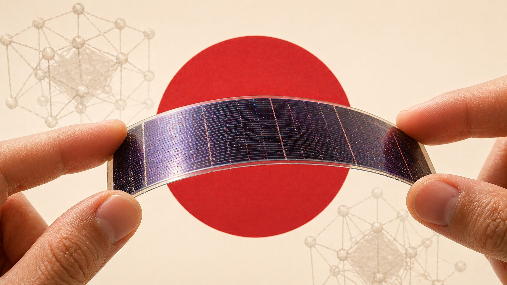
Today, Japan holds a 50%+ global share in semiconductor materials. For specific high-end segments like EUV photoresists, that share is near 100%. You cannot print a chip at TSMC without Shin-Etsu Chemical. You cannot coat a wafer without Tokyo Electron. You cannot cut a silicon ingot without Disco Corporation. Japan has an oligopolistic grip on these key areas.
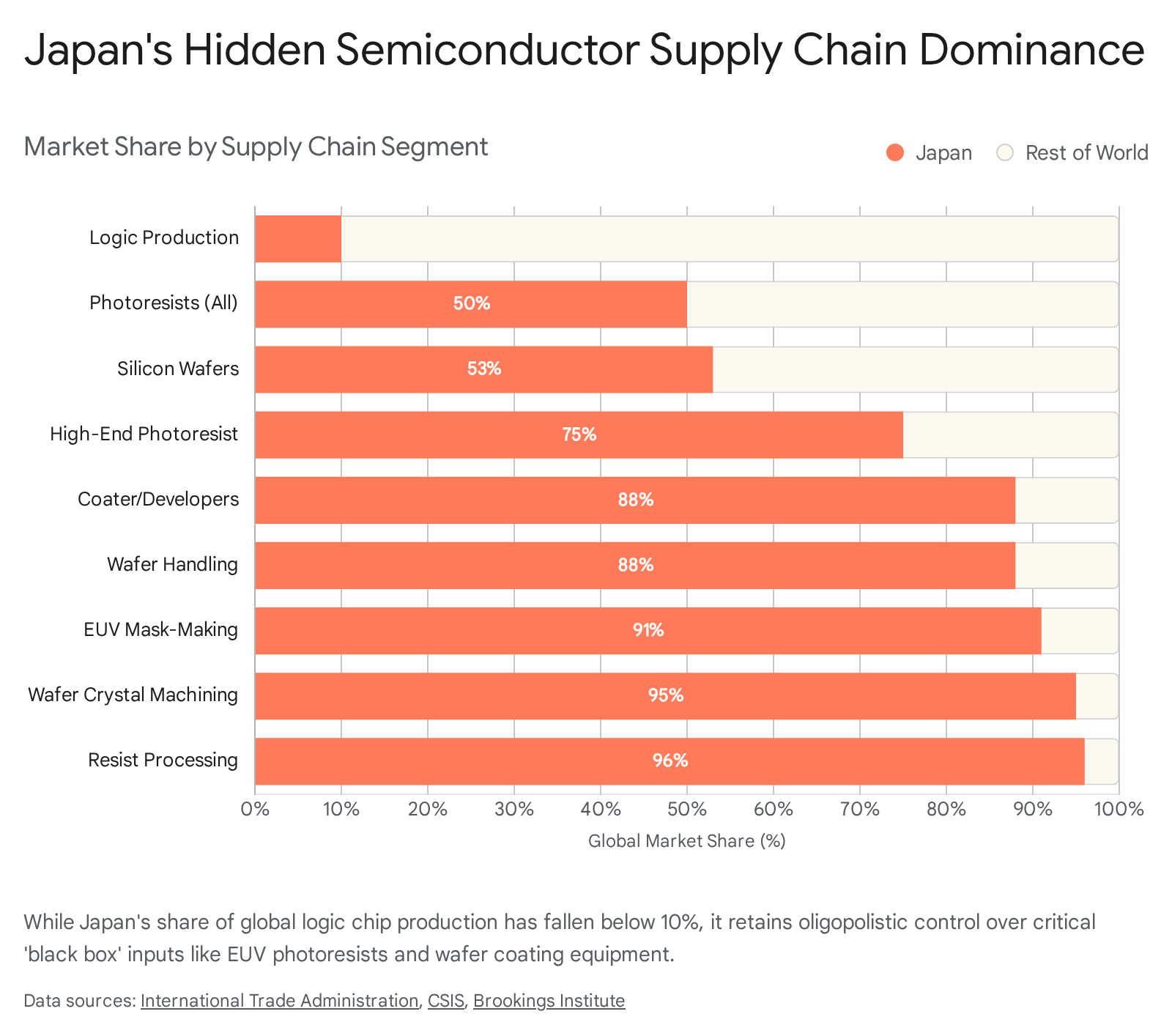
The mistake is assuming that because Japan lost the B2C chip war, it lost the capability. It didn’t. The “muscle memory” of precision engineering is still there, locked inside these materials companies. The Rapidus project is essentially an attempt to unlock that latent capability and re-apply it to logic manufacturing.
Taiwan Just-in-Time, Hokkaido Just-in-Case…
Why now? Why is the Japanese government suddenly pouring trillions of yen into a sector it ignored for two decades?
The answer is fear. Or, more precisely, the pricing of systemic risk.
For forty years, the global semiconductor supply chain was optimized for efficiency. “Just-in-Time” was the religion. It didn’t matter where the chips were made, as long as they were cheap and reliable. This logic concentrated 90% of the world’s advanced computing power on an island that China claims is a renegade province.
Then came COVID. Then came the chip shortages that forced Toyota to halt production lines. Then came the realization in Washington and Tokyo that if the Taiwan Strait closes, the global economy stops. We moved from “Just-in-Time” to “Just-in-Case.”
The “Silicon Shield,” the theory that Taiwan is too valuable to invade, is inverting. The concentration of capacity in Taiwan is now seen as a liability. The US CHIPS Act was the first response: bring manufacturing back to American soil. But the US lacks the ecosystem. It has the designers (Nvidia, Apple) but it lost the Monozukuri. TSMC’s struggles in Arizona, such as labor shortages and culture clashes, are a testament to how hard it is to transplant a manufacturing culture.
TSMC’s overseas projects provide an A/B test in plain sight. TSMC announced its Kumamoto fab in October 2021 and reached mass production in December 2024 (~38 months), while its Arizona fab was announced in May 2020 and is only reaching initial production in early 2025 (~57 months), about 50% slower despite heavier subsidies and political backing.
Japan represents the “friend-shoring” arbitrage. It is a US ally. It has a stable political system. It has a weak yen (making investment cheap). And unlike the US, it has a workforce that culturally understands the rigors of semiconductor manufacturing.
Rapidus = Fast
Rapidus is the Japanese government’s moonshot. The goal is to mass-produce 2-nanometer chips by 2027.
For context, the most advanced chips made in Japan today are 40-nanometer logic chips, technology from fifteen years ago. Rapidus aims to skip 20 years of development in 5 years.
But the Rapidus thesis is not about beating TSMC on volume. It is about beating them on speed.

TSMC is a volume monster. Their business model relies on massive batches and long lead times (Turnaround Time, or TAT). It takes about 120 days to process a wafer through a modern fab. TSMC is optimized for Apple: selling 100 million iPhones. It is not optimized for a startup needing a specialized AI accelerator tomorrow.
Rapidus is building a “Short TAT” foundry. Their target is to cut that 120-day cycle to 50 days, or even 15 days for “hot lots”.
How? By using single-wafer processing instead of batch processing.
In a batch process, you put 25 wafers in a boat and process them together. It’s efficient, but if you have a defect, you lose the whole batch. Single-wafer processing treats every wafer individually. It’s slower for massive volume, but it allows for incredibly fast feedback loops and customization. You get data from every single wafer, instantly.
This is a fundamental divergence in philosophy. TSMC is optimized for throughput. It is the supertanker of the industry, unbeatable on volume and cost for massive runs. Rapidus is optimized for latency. It is the speedboat, designed to turn designs into silicon in record time.
This aligns perfectly with where the market is going. The AI era is fracturing the semiconductor market. We are moving from general-purpose CPUs (Intel) to domain-specific architectures (ASICs, NPUs). The future belongs to companies like Tenstorrent (which has already partnered with Rapidus) who need specialized chips, fast. They don’t need 100 million units. They need fast iteration.
It’s All About the People
The biggest headwind for Japan is typically talent. The engineers who built the 1980s dominance are retiring.
But Rapidus is executing a clever arbitrage here: Repatriation.
They are not just hiring fresh grads. They are hiring the “Last Vanguards.” These are the engineers in their 50s and up who worked in the golden age of Toshiba and Hitachi, then left for the US or worked in the shadows when the Japanese industry contracted. These are “battle-ready” troops. They possess the implicit knowledge of physics and chemistry that you cannot learn from a textbook.
Simultaneously, they are sending hundreds of younger engineers to Albany, New York, to train with IBM. This is the “Titans” project.

The deal with IBM is key. IBM invented the 2nm Gate-All-Around (GAA) technology. This is the holy grail of transistor architecture: nanosheets that allow for better power control than the current FinFET standard. But IBM has no fabs; they sold them to GlobalFoundries years ago. IBM needs a manufacturing partner to realize its IP. Rapidus is that partner.
This is a symbiotic relationship. IBM provides the IP. Japan provides the Monozukuri discipline to scale it.
Why Hokkaido?
Why build this in Chitose, Hokkaido? Why not Kyushu, where TSMC is building its fab? Why not the industrial heartland of Aichi?
The answer lies in Water, Power, Lifestyle, and Protection.
Semi Fabs Are Thirsty
Semiconductor fabs drink water. A lot of it. A single advanced fab can consume millions of gallons of ultra-pure water a day. TSMC’s expansion in Taiwan has been plagued by severe droughts, forcing the government to truck in water and halt irrigation for farmers. Kyushu has water, but it is becoming crowded with TSMC’s arrival.
Hokkaido is the “Alaska of Japan.” It is awash in fresh, clean water. The Chitose River provides an abundant industrial water source that is chemically ideal for cleaning wafers. In a world of water scarcity, Hokkaido offers a security premium that Taiwan cannot match.
Semi Fabs Need Energy
We are moving into an era where energy density matters. But it’s not just about “renewables.” It’s about stable, clean baseload power.
Hokkaido has a unique energy portfolio. Yes, it has the highest potential for solar and wind in Japan. But more importantly, it has the Tomari Nuclear Power Plant. The Hokkaido Governor recently signaled willingness to restart the plant. A restart of Tomari would provide the massive, carbon-free baseload power required to run a 2nm fab 24/7 without relying on imported fossil fuels.
Combined with the region’s immense geothermal potential (ranked 2nd in Japan), Hokkaido is positioning itself not just as a “green” hub, but as a “clean energy fortress.” In Tokyo or Osaka, the grid is constrained. In Hokkaido, the combination of nuclear, geothermal, and solar offers a path to energy sovereignty that is critical for a strategic asset like a fab.
Semi Engineers Need Lifestyle
Chitose is next to Sapporo. Chitose hosts the island’s largest airport, so engineers and customers can fly in and out on a moment’s notice. You don’t have issues like smog in Beijing or poop in San Francisco. You have powder snow, incredible food, and affordable housing.
Japan is trying to sell a lifestyle to engineers. If you are a top chip designer in Silicon Valley, moving to Tokyo could be a shock: tiny apartments, crowded trains. Moving to Hokkaido? That’s a ski chalet with gigabit fiber.
Rapidus calls this the “Hokkaido Valley” vision. It is an attempt to create a cluster that rivals Hsinchu in Taiwan or Grenoble in France, but with a quality of life that attracts the global elite.
Semi Fabs Need Protection
Finally, Hokkaido is geographically removed from the immediate geopolitical tensions of the Taiwan Strait and the seismic risks that plague the rest of Japan.
Located roughly 1,500 miles from the flashpoints of the First Island Chain, the island offers a secure “backup drive” for the Western alliance. Domestically, the Chitose area sits on geologically stable ground with a relatively low risk of major earthquakes compared to the industrial belts of Tokyo or Kyushu, providing the necessary stability for the atomic-level precision required in 2-nanometer manufacturing.
There is also a “hard power” dimension to this choice; the Rapidus fab is being built immediately adjacent to the Chitose Air Base, home to the Japan Air Self-Defense Force’s 2nd Air Wing.
This proximity simplifies physical security against modern threats like drones and underscores the dual-use strategic nature of the technology. By intertwining this military-grade security with direct access to New Chitose Airport for rapid global logistics, Rapidus is not merely a commercial venture, but a fortified national asset designed to ensure the continuity of the digital world even if geopolitical tensions in East Asia boil over.
Japan is Back
Ultimately, Japan’s semiconductor revival is not a nostalgic attempt to recreate the sheer volume of the 1980s, but a strategic evolution designed for the reality of the 2020s. The nation has successfully pivoted from the brittle dominance of final assembly to the antifragile hegemony of the supply chain, and now, with Rapidus, it is closing the loop. By marrying its stranglehold on the “black box” materials of chipmaking with a new, agile manufacturing philosophy, Japan is transforming from a legacy competitor into an indispensable partner.
To be sure, the hurdles remain immense. Jumping from 40-nanometer legacy nodes to 2-nanometer frontier tech is akin to learning to fly by piloting a rocket, and the graveyard of state-backed tech consortia is vast.
Yet, the cost of failure for Japan is merely financial, while the cost of inaction for the global order is existential. In an era where “efficiency” has been replaced by “resilience” as the primary virtue of supply chains, the Rapidus project is not just a commercial gamble; it is a geopolitical insurance policy. The West doesn’t just need a faster chip; it needs a safer one, and the market is finally pricing in the premium of political stability.
As the construction cranes rise above the snowy plains of Chitose, they signal a shift in the center of gravity for the digital age. Japan has awakened from its “Galapagos” slumber not to find itself obsolete, but to find that the world has circled back to value exactly what it offers: precision, stability, and trust.
The narrative that Japan lost the semiconductor war was premature; it was simply playing a longer, quieter game. The sun isn’t setting on Japanese tech; it is rising in the North, illuminating a new “Silicon Archipelago” ready to serve as the hardened backup drive for global democracy.